Huawei unveiled its most aggressive semiconductor gambit yet on Monday, revealing a new “LogicFolding” chip architecture that could let it compete with TSMC’s cutting-edge 2nm process by 2031—despite being blocked from Western equipment and facing U.S. sanctions that have already forced Nvidia to cede the Chinese smartphone market to its rival.
How Huawei‘s ‘LogicFolding’ Could Reshape the Chip War
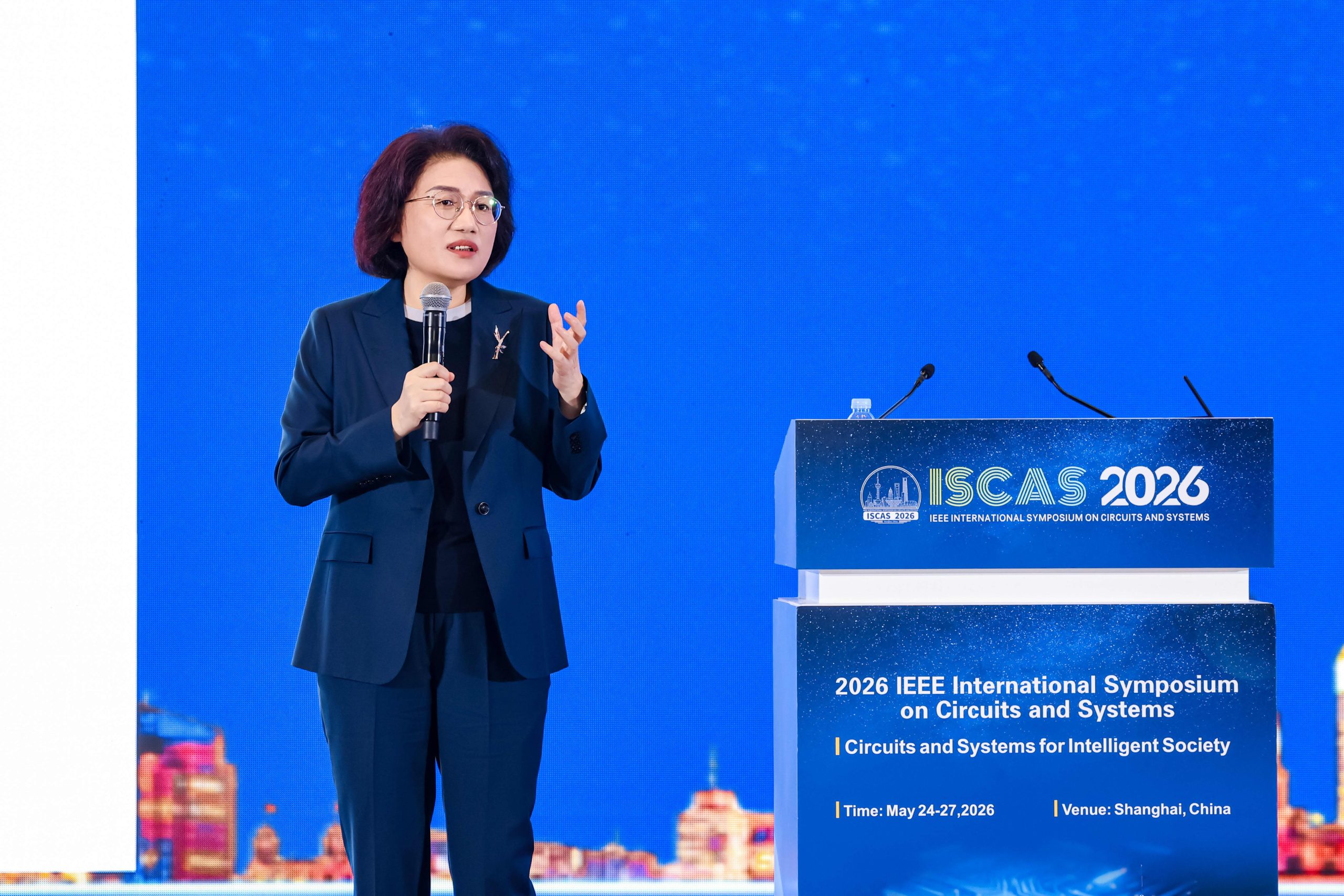
At the 2026 IEEE International Symposium on Circuits and Systems in Shanghai, Huawei’s semiconductor president Tingbo He presented the company’s “Tau (τ) Scaling Law,” a radical departure from Moore’s Law that replaces geometric shrinking with a focus on compressing signal propagation delays. The result? A folded-chip architecture Huawei claims could deliver performance equivalent to 1.4nm-class manufacturing—while TSMC has only just begun volume production of its 2nm chips.

This isn’t just a theoretical breakthrough. Huawei plans to deploy LogicFolding in its next-generation Kirin smartphone chips this fall, with the Mate 90 series serving as the first consumer testbed. The stakes couldn’t be higher: Nvidia CEO Jensen Huang told CNBC last week that his company had “conceded” the Chinese market to Huawei, citing U.S. export restrictions that have blocked advanced chips like the H200 from reaching China.
“For Nvidia, this means the window to sell advanced chips such as the H200 into China is narrowing.”
The timing is electric. While Huawei’s Mate 60—launched in 2023—helped the company claw back smartphone market share from Apple using 5G chips, the new LogicFolding approach targets AI and high-performance computing, where the U.S. has maintained tighter controls. The company’s ambition to match TSMC and Intel by 2031 would mark a seismic shift in global semiconductor dominance.
The Physics of a Folded Future
Huawei’s τ Scaling Law isn’t just about smaller transistors—it’s about rethinking how chips are physically assembled.

- Device level: Optimizing transistor resistance and parasitic capacitance to minimize time constants.
- Circuit level: “LogicFolding” architecture breaks traditional layout boundaries, shortening critical-path wiring and reducing signal propagation delays.
- Chip level: Full-stack coordinated design for workload-driven instruction/data flow control.
- System level: UnifiedBus protocols to slash memory access latency in AI clusters.
In practice, this means stacking and folding chip layers to achieve density gains without relying on extreme ultraviolet (EUV) lithography—the same Dutch-made ASML machines Huawei has been denied access to under U.S. sanctions. But experts warn the approach isn’t without risks. Paul Triolo of DGA Group cautioned that “a stacked/folded design can produce effective density gains, but it does not mean Huawei has solved the full process, yield, power, thermal, and device-performance problems associated with true 1.4nm-class manufacturing.”
“A stacked/folded design can produce effective density gains, but it does not mean Huawei has solved the full process, yield, power, thermal, and device-performance problems associated with true 1.4 nm-class manufacturing.”
The thermal and packaging challenges are particularly acute. Neil Shah of Counterpoint Research noted that “this parallel semiconductor path is still unproven at scale,” with potential manufacturing yields hit by “tough thermal constraints and packaging complexities.” The first real test will come with the Mate 90 series, but scaling this to AI data centers—where Nvidia currently dominates—would be the ultimate litmus test for China’s semiconductor ambitions.
Washington’s Dilemma: Can Huawei Really Compete?
The U.S. response to Huawei’s breakthrough will be critical. While the company has made progress with its homegrown Kirin chips, its ability to compete in AI and high-performance computing remains untested. The Biden administration has already restricted Huawei’s access to advanced chipmaking equipment, and any perceived progress could trigger further sanctions.
Yet the geopolitical implications are enormous. If Huawei succeeds in closing the gap with TSMC, it could force the U.S. to reconsider its semiconductor export policies—or risk accelerating China’s technological self-sufficiency. The company’s academic ambitions, including seeking greater recognition for its semiconductor research, signal a long-term play to build credibility in the global tech community.
What’s Next: The 2031 Horizon
Huawei’s roadmap is aggressive. By 2031, the company aims to deliver performance equivalent to 1.4nm-class chips—just as TSMC begins volume production of its next-generation 2nm process. The question is whether LogicFolding can deliver on its promises at scale.

For now, the focus is on consumer electronics. The Mate 90 series will be the first public test of Huawei’s folded-chip architecture, with AI capabilities likely to be a key differentiator. If successful, this could force Apple and other smartphone makers to rethink their chip strategies—or risk losing ground in China’s massive market.
The real battle, however, will be in AI and data centers. Nvidia’s dominance in these areas has been a cornerstone of U.S. tech leadership, and Huawei’s push into this space could trigger a new front in the chip war. With the U.S. already struggling to maintain its edge in semiconductor manufacturing, Huawei’s progress—however incremental—could accelerate a dangerous technological decoupling between Washington and Beijing.
One thing is certain: the semiconductor industry’s future will no longer be guided by Moore’s Law alone. Huawei’s τ Scaling Law represents a bold bet that time—and not just space—can drive the next wave of computing innovation. Whether it pays off remains to be seen.
